
Description
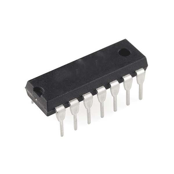
CD4015 – Dual 4-bit Static Shift Register
The CD4015 is a dual 4-bit static shift register IC, meaning it can shift data in or out serially or store data in parallel. This chip is part of the CD4000 series of CMOS logic ICs, which are designed for low power consumption and high noise immunity.
It is a commonly used device in digital circuits where data needs to be shifted or stored, and it can function both in serial-to-parallel and parallel-to-serial modes. The CD4015 is typically used in applications such as data storage, data transfer, serial communication, LED displays, and timing circuits.
Key Features:
- Dual 4-bit Register:
- The IC contains two independent 4-bit shift registers, which allows for dual-channel operation. Each register can hold 4 bits of data, providing a total of 8 bits of data storage.
- Shift Register Mode:
- The CD4015 can shift data serially (bit by bit) either into or out of the register. This makes it useful for transferring data across fewer pins or for serial communication purposes.
- Parallel Loading:
- The shift register supports parallel loading, meaning you can load the shift register with 4 bits of data at once through parallel inputs.
- Shift Right and Shift Left:
- Data can be shifted in both directions (right and left) using dedicated control pins, providing flexibility for various data manipulation applications.
- Clear Function:
- The clear (reset) pin allows you to reset the register, clearing the stored data (all bits set to zero), ensuring a predictable state before shifting or storing new data.
- Low Power Consumption:
- Like most CMOS devices, the CD4015 is designed to consume minimal power, making it suitable for battery-powered or low-energy circuits.
- Flexible Logic Levels:
- The CD4015 works with logic levels compatible with the CMOS family, allowing for compatibility with other CMOS devices.
- High Noise Immunity:
- CMOS technology provides the IC with high noise immunity, making it reliable for operation in noisy environments.
Applications:
- Data Shift and Transfer:
- The CD4015 can be used in systems that require data shifting or serial-to-parallel conversion, such as communication protocols or digital data transfer.
- LED Displays:
- It can be used to control LED displays by shifting bits of data to control which LEDs are lit, especially in multiplexed LED arrangements.
- Signal Processing:
- The chip can be used in signal processing circuits that require shifting or delaying bits of data.
- Timing and Control Systems:
- It is often used in timing circuits or sequential logic applications where specific timing or data shifting is needed to drive other logic circuits or components.
- Serial-to-Parallel and Parallel-to-Serial Data Conversion:
- The IC is ideal for applications requiring conversion between serial data and parallel data, such as in serial-to-parallel or parallel-to-serial data converters.
- Control Applications:
- It can be used in control applications where multiple devices need to be controlled by shifting data bit by bit to a group of output devices.
- Data Storage:
- In temporary data storage applications, the CD4015 can store data and be used to read/write this data through shifting.
Pinout Configuration (16-Pin DIP Package):
- Pins 1-4 (Shift Register 1 – Parallel Data Inputs):
- These pins are for the parallel loading of data into the first shift register.
- Pin 5 (Shift Left/Right Control – Register 1):
- This pin determines the shift direction for the first register.
- Pin 6 (Shift Clock – Register 1):
- This pin is used to clock the data into or out of the first register.
- Pin 7 (Output – Register 1):
- This pin outputs the data stored in the first shift register.
- Pin 8 (Clear/Reset):
- When activated, this pin resets the contents of both shift registers to zero.
- Pins 9-12 (Shift Register 2 – Parallel Data Inputs):
- These pins are for the parallel loading of data into the second shift register.
- Pin 13 (Shift Left/Right Control – Register 2):
- This pin determines the shift direction for the second register.
- Pin 14 (Shift Clock – Register 2):
- This pin is used to clock the data into or out of the second register.
- Pin 15 (Output – Register 2):
- This pin outputs the data stored in the second shift register.
- Pin 16 (Vcc):
- Power supply pin (typically 5V for CMOS logic ICs).
Operating Modes:
- Serial Input:
- Data can be shifted into the registers one bit at a time from the serial input pin.
- Parallel Input:
- Data can be loaded directly into the registers all at once via the parallel input pins.
- Shift Direction:
- The shift direction can be controlled using a dedicated control pin (Shift Left/Right). This allows you to shift the stored data either to the left or right in the register.
- Clocking:
- The clock pin is used to control the timing of the shifts. A clock pulse will shift the data in or out of the register. The data is shifted either left or right depending on the control pin settings.
- Clear Function:
- The reset pin clears the contents of the shift registers, setting all bits to zero. This is useful when you need to initialize the shift register before starting a new operation.
Advantages:
- Dual 4-bit Registers:
- The CD4015 provides two 4-bit shift registers in a single IC, which is useful for applications that need to handle two independent data streams.
- Low Power:
- Like other CMOS devices, the CD4015 is very energy-efficient and works well in low-power circuits.
- Flexibility:
- The shift registers can be used for both serial-to-parallel and parallel-to-serial data transfer, which adds to the versatility of the device.
- Ease of Use:
- The IC provides simple control pins for shifting, clocking, and clearing, making it easy to integrate into a wide range of digital projects.
- High Noise Immunity:
- Being a CMOS IC, it offers good noise immunity, ensuring stable operation even in noisy environments.
Disadvantages:
- Limited Data Length:
- Each register only holds 4 bits, so the total storage is limited to 8 bits in total (for both registers). If more bits are required, additional shift registers or memory ICs may be needed.
- Clock Dependency:
- The operation of the shift register depends on the clock signal. If the clock is unstable or inconsistent, the data transfer may be affected.

Reviews
There are no reviews yet.