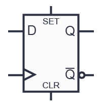
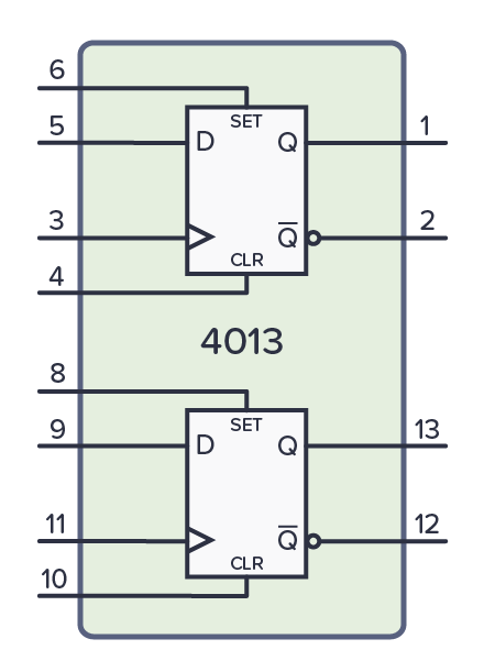
The CD4013 contains two D flip-flops. A D flip-flop stores a 1-bit value and only changes when it receives a clock signal. Specifically, its output pin (Q) changes to whatever is on the input pin D (data) when the clock (CLK) pin goes from LOW to HIGH.
Pin Overview
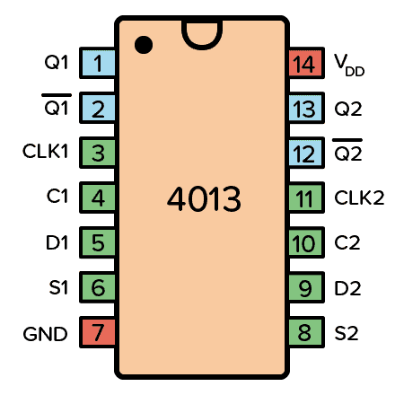
CD4013 Pinout
Pin Name
Pin #
Type
Description
VDD
14
Power
Supply Voltage (+3 to +15V)
GND
7
Power
Ground (0V)
Q1, Q2
1, 13
Output
Outputs from the two D Flip-Flops
Q1, Q2
2, 12
Output
Inverted outputs from the two D Flip-Flops
CLK1, CLK2
3, 11
Input
Clock input for the two D Flip-Flops (Rising Edge)
D1, D2
5, 9
Input
D (data) input for the two D Flip-Flops
S1, S2
6, 8
Input
Preset the Flip-Flop output to 1
C1, C2
4, 10
Input
Reset the Flip-Flop output to 0
Pin overview for the 4013 IC
What is a D Flip-Flop?
A D flip-flop is a circuit that can store one bit of data. Its output can either be HIGH or LOW. The output changes to whatever is on the data (D) input when the clock goes from LOW to HIGH. Also called on the rising edge of the clock. (Some D flip-flops change on the falling edge instead.)
This means that the D flip-flop only cares about what is on the data (D) input at the moment this transition happens.
Some D flip-flops have an inverted clock input, which means the output only changes when the clock goes from HIGH to LOW. This is called on the falling edge.
The D flip-flops in the CD4013 also have Set (S) and Clear (C) pins. These can be used to either set the output to HIGH or reset it to LOW, independently of the clock.
A D flip-flop is often used to create shift registers and binary counters, frequency dividers, simple toggling circuits, and much more. See the circuit example further down for a specific use case.
The D (data) pin is where you input the data you want to store in the flip-flop.
Provide a rising edge signal (a signal going from LOW to HIGH) on the CLK pin to store the data from the D pin to the output pin Q.
The output pin Q is always the opposite of pin Q.
Use the S (set) pin to force the output pin HIGH.
Use the R (reset) pin to force the output pin LOW.
The two D flip-flops in the 4013 chip and their pin numbers
Alternatives and Equivalents for CD4013
You likely find the 4013 IC marked as CD4013, NTE4013, MC14013, HCF4013, TC4013, or HEF4013. Usually with a few extra characters at the end (Ex: CD4013BE).
This has to do with the manufacturer of the chip and the technology used. But the functionality and the pins are the same.
Or try one of the following IC alternatives with D flip-flops:


Reviews
There are no reviews yet.